For more than 50 years, Moore’s law has successfully described the steadily increasing power of microelectronics. Decades of exponential growth in transistor density has revolutionized the way humanity lives, and has generated a worldwide semiconductor industry. However, as Gordon Moore, co-founder of Intel and author of Moore’s Law, once said: “no exponential is forever.” Today, the imminent end of classical Moore’s Law scaling represents a major turning point in the history of microelectronics. The authors explore the historic background of Moore’s Law, the economic implications of its demise, and policy ideas for the US Department of Defense to adapt to this paradigm change.

The End of Moore’s Law
With over 50 years of sustained exponential scaling, the field of microelectronics has had a profound impact on society. In the 1960s, electronic chips had but a handful of components; today, a single chip contains several billion transistors. Moore’s law has characterized a $336 billion worldwide semiconductor industry,1 and has fed the development of multiple other industries. From modern GPS applications, to smart phone technology, it has revolutionized the way we live. Microelectronics has driven the historic transformation from analog to digital representation of data, and has enabled the vast expansion of data storage.
However, the heady days of exponential scaling are about to come to an end. Fundamental limits signal a major paradigm shift in microelectronics technology. These changes will be disruptive to the industries that have grown accustomed to exponential growth as described by Moore’s Law. The US Department of Defense will need to adapt its policies to ensure continued technological superiority.
Moore’s Law, as formulated by Gordon Moore in his 1965 paper “Cramming More Components onto Integrated Circuits,” is nothing more than an empirical observation that the density of components in an integrated circuit (IC) doubles every 18-24 months. According to Moore,2
…the complexity for minimum component costs has increased at a rate of roughly a factor of two per year. Certainly over the short term this rate can be expected to continue, if not to increase. Over the longer term, the rate of increase is a bit more uncertain, although there is no reason to believe it will not remain nearly constant for at least 10 years.
In 1975, Moore updated this prediction to expect the doubling of transistors every two years. Transistor density has in fact continued to increase, doubling every 18 to 24 months since 1975, with a number of other parameters also changing in the positive direction. The result has been that devices have become faster, more reliable, efficient, and cheaper to produce. There has been much speculation as to the longevity of Moore’s Law. Moore himself only expected the law to last for 10 years, but since 1965, we have seen 50 years of exponential growth.
Yet in the early 2000s, cracks began to appear. An upper limit on processor speeds appeared, due to challenges in reducing levels of power consumption (and thus increasing heat dissipation). Multi-core processors were introduced, but required parallel computing to achieve performance gains; yet typical applications, such as operating systems, cannot be perfectly parallelized because many of the steps in a program depend on the results of earlier steps. The increasing difficulties with technology feature size scaling were also reflected in higher fabrication process complexity. Advancements in photolithography, the technology required to fabricate integrated circuits, stalled at a wavelength of 193 nm. This has necessitated costly imaging “tricks” and multiple photolithographic exposures per level, slowing down the fabrication rate and adding cost.
Currently, in 2015-2016, even more serious limits have been reached. With transistor minimum feature sizes falling to 14 nanometers, the industry has reached a size regime where a countable number of atoms comprise each component within the IC, presenting difficulties in process control. The evidence that a fundamental limit has been reached is apparent in the actual cost per component. A major turning point has recently been realized as the cost per transistor on an IC has started to increase after 28nm. As shown in Figure 1, this change is the first time this has happened in the past fifty years, representing a major shift for the future.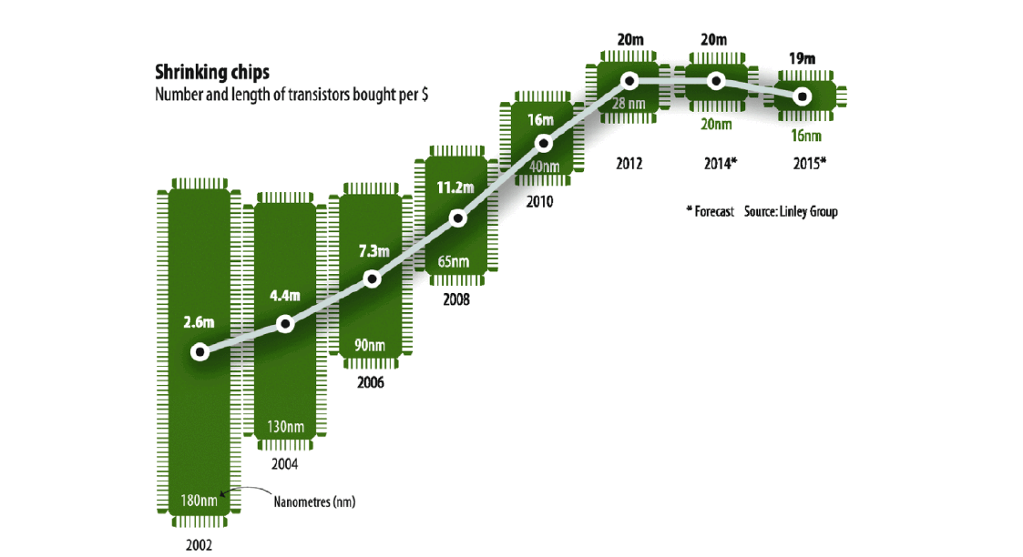
Figure 1. Increasing cost per transistor after the 28 nm node. Source: The Linley Group, 2013.
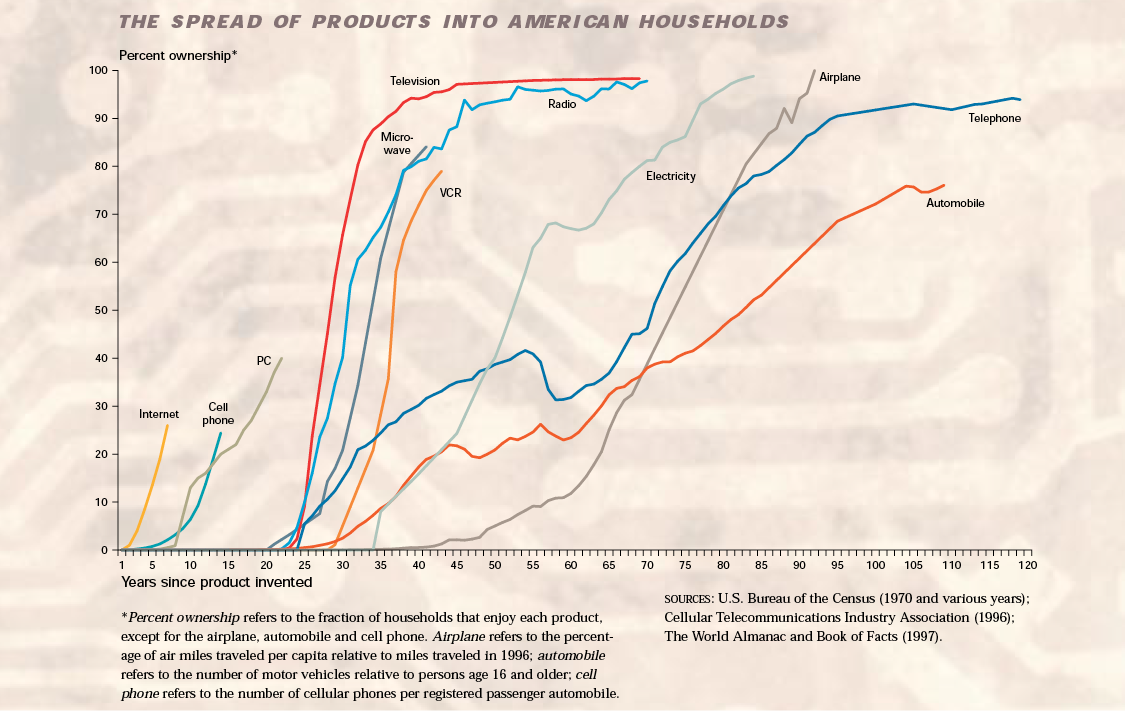
Figure 2. The spread of products into American Households. Reprinted here with permission, Federal Reserve Bank of Dallas 1996 Report, by W. Michael Cox and Richard Alm.
Consumer Product Dominance
In the beginning, the microelectronics industry was fueled by government investments, much of it through the US Department of Defense (DoD). DoD’s expenditures in equipment as well as research and development (R&D) in electronics was in the billions of dollars, increasing from $3.2 billion in 1955 to $7.8 billion in 1964 – a significant investment considering that this took place more than fifty years ago.3 DoD spurred integrated circuit development and production in order to increase the automation, miniaturization, and reliability of defense systems. Military specific (or MIL-spec) components were also developed, with the added goal of ensuring that parts used in military systems maintained the functional capability and reliability to operate in harsh environments.4 DoD also wanted multiple sources of chips, and so encouraged technology transfer between semiconductor firms, which indirectly grew the product diversity of the semiconductor industry.5 Since then, DoD’s influence over the semiconductor market has waned.
Semiconductors became more and more dominated by commercial applications, evidenced by the military’s falling share of the US market from nearly 100% in 1962 to roughly 30% by 1968.6 After 1970, commercial IC applications totally dominated. Microelectronics became a “commodity,” feeding interchangeably many different commercial applications, as well as the military’s needs. Growing consumer demand established a sizable market for increasingly sophisticated microelectronics. From the 1980s through the 1990s, a prime driver was the personal computer. From the 2000s to the present, the primary driver has been the mobile communications market, as exemplified by the cell phone. The economic “engine” of the microelectronics industry has been built on the “fuel” of very high volume consumer applications.
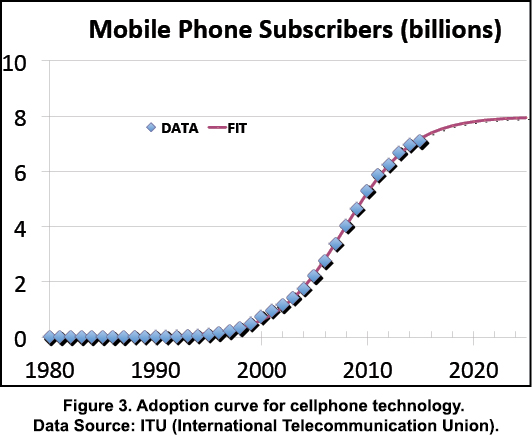
A potential challenge to the consumer demand trend is the “adoption curve” of new technologies, signifying how quickly they penetrate a national or worldwide market. Figure 2 shows that older technologies such as the car, telephone, and household electricity took many decades to become ubiquitous, whereas newer technologies like the TV and VCR only took a few years to saturate the global market. A seen in Figure 3, even the current cell phone market is showing evidence of saturation.
For the past few decades, Moore’s Law has guaranteed the rapid obsolescence of most consumer electronic devices. Accordingly, most consumers felt compelled to replace their PCs every few years, and even faster refresh cycles for smart phones became commonplace. Rapid penetration of electronic devices throughout the entire world further propelled the microelectronics industry.
Contrastingly, DoD has been challenged by the fast lifecycles of consumer products, compared to the much slower acquisition cycles of typical military systems. Moreover, the commercial industry drove the types of ICs that were produced, with a relatively small number of “general-purpose” ICs made to meet the demands of most consumer applications. As a result, DoD had to adapt its systems to piggyback on available commercial microelectronics; military systems used expensive specialized components only when absolutely necessary.
As the consumer market grew to a global size, economies of scale could be reached by achieving very high volume production of relatively standardized ICs. Industry R&D focused on technologies to maximize volume and yield, in addition to shrinking size and increasing performance. Business boomed as consumer products were regularly upgraded by taking advantage of steadily increasing performance. Even though DoD had driven much of the early development of the technology, its demands were overshadowed by the burgeoning commercial marketplace and eventually its role was primarily limited to adapting commercially available products.
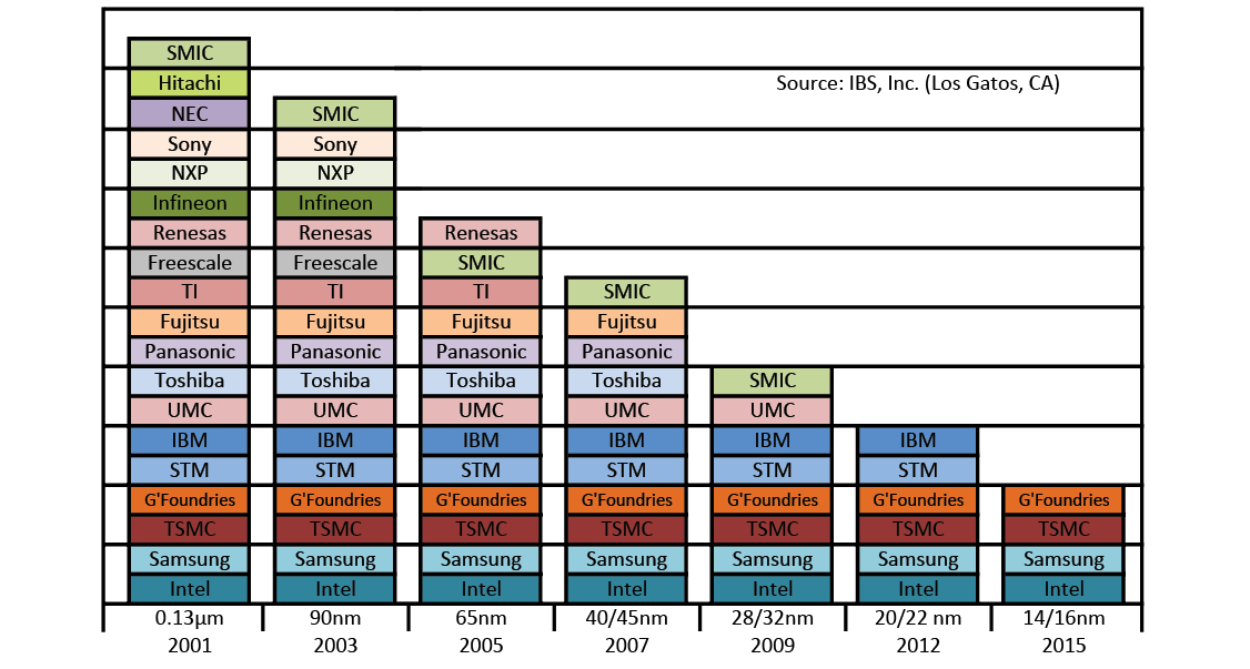 Figure 4. Dramatic Consolidation of state of the art CMOS Fabs. Source: IBS , Inc. (Los Gatos, CA).
The Economic Drivers
With the demise of Moore’s Law, what will fuel the microelectronics engine? How will the microelectronics industry adapt?
Already, we see changes in the way the industry operates. Recently there has been a dramatic increase in mergers and acquisitions among the larger manufacturing companies.7 Further, as shown in Figure 4, there has been a stark decline in the number of microelectronics fabrication facilities (or fabs) capable of manufacturing state-of-the-art chips.
A new product class could create a renewed driver of the current industry model. The future highly interconnected world, known as the “Internet of Things” or IoT, will certainly require many electronics parts. However, the parts needed for IoT devices generally will not require powerful processing. They will also need to be cheap, durable, and use low power. It is not likely that this market will be enough to sustain the current microelectronics business model of high volume manufacturing of complex ICs. Without a new high volume commodity product, such as a replacment of the smart phone, the microelectronics industry will need to evolve in significantly new ways.
Without plentiful “fuel” in the form of Moore’s Law coupled with high volume commodity consumer products that customers want to frequently upgrade, the microelectronics industry will lose the economies of scale required to produce complex ICs at attractive prices. Consumers will keep their technology products for longer periods, placing a greater emphasis on their reliability and sustained utility. The microelectronics inside of products will migrate from “commodity” items to “durables,” like consumer appliances.
Once market saturation occurs, a technology industry typically matures to serve the unique needs of its customers. Business differentiators that offer a range of different amenities to serve unique needs are found in the aviation industry, for example,8 as well as the automobile industry. Saturation in the microelectronics industry, if it occurs, will have major impacts on the way the business is structured. In the future of integrated circuits, a new emphasis will be put on meeting a wide variety of needs of customers via customization of features for specialized markets – and DoD will likely return as a driver of some of these markets. Thus, DoD needs to be prepared to leverage these new industry dynamics.
Future Directions
In a new world of microelectronics as durables, the key driver of innovation and performance may revert back to military and aerospace applications. DoD may once again be in the captain’s chair, at least for their particular needs. The defense community has always been willing to pay a premium for required critical performance, but had become a sideline customer during several decades of the microelectronics “commodity” phase. In the new commercial environment for microelectronics, specialized technologies carrying a cost premium will mostly likely be driven once again by DoD’s applications for the warfighter. The microelectronics research agenda could once again be driven by specialized customers, and DoD can steer development in directions that meet its needs for technical superiority in military applications.
One of the promising “Post-Moore” emerging technologies that might become important to DoD is 3-Dimensional (3D) stacking, also called 3DIC technology. 3D stacking is a promising means to achieve high performance custom ICs, without requiring a greater number of transistors in two dimensions. A schematic of this approach is shown in Figure 5. The key to 3DIC technology is the ability to integrate multiple active “tiers” into a final customized IC. Each individual tier can be implemented in a different specialized technology. Designers can combine sophisticated processors with sensor tiers, or even tiers at legacy technology levels, in such a way that as to maximize security and reliability in addition to increasing performance. At this point in time, supporting infrastructure is lacking, including robust design tools and supply chains to provide tiers and interconnects. This infrastructure will not be developed by industry in the absence of an obvious high volume commodity driver. DoD can therefore play an important role helping to develop the enabling infrastructure of 3DIC technology, reaping the custom performance benefits as well as helping seed a new US manufacturing industry.
Another enabling technology that could benefit DoD is based on the paradigm of low volume flexible fabrication. As noted earlier, commercial microelectronics rely on high volume fabrication to realize economies of scale, and as a result the available types of ICs are limited. Going forward, flexible low volume approaches will play an increasingly important role in providing customized parts for specialized applications. Such fabrication approaches are based on a different type of economic model. In this model, specialty or “custom” parts are the goal, and absolute lowest cost per part is not a requirement. Such an approach is already practiced in some domains where aggressive scaling is not required, such as radio-frequency and radiation-hardened parts. This new business model will need to be able to support higher cost margins than today’s typical commercial manufacturing. The low volume flexible fabrication paradigm also requires alternative approaches to ensuring reliability, including more robust testing. DoD can therefore play an important role in developing the infrastructure required, such as multi E-beam Direct Write technologies. Such an investment would provide desired custom parts for the DoD as well as helping seed a new US manufacturing industry.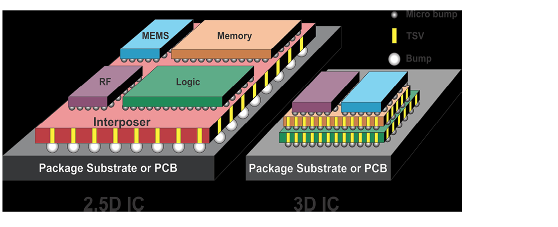
Figure 5. Two main types of 3DIC technologies. On the left is an “interposer” based solution and on the right is a 3D-stacked “multi-tier” solution featuring a higher density of vertical interconnects. Reprinted here with permission, Dr. Bob Patti of Tezzaron/Novati.
Conclusion
The impending end of Moore’s Law represents much more than a technological paradigm shift. This major turning point will in fact trigger major changes in the business models of the microelectronics industry. Recent decades have been characterized by commodity consumer products like the PC and cell phone, with product generations that were refreshed rapidly as microelectronics technology advanced. As these markets saturate, a new business model is required for the industry and more emphasis will be placed on reliability and robust lifetime performance. More attention will also be placed on customized performance for smaller market segments, as opposed to a “one size fits all” generic approach. This “maturing” of the microelectronics industry will follow a progression similar to past technologies, such as cars and commercial aviation. As a result of this change, new fabrication approaches will become more important including 3DIC integration and low volume flexible fabrication concepts. The DoD can play a key role helping to develop the engineering techniques and the infrastructure for these new technologies. This will not happen automatically by industry given the business uncertainties and risks that accompany the end of Moore’s law. This major paradigm change offers the DoD another opportunity to help drive microelectronics to both serve its specialized needs and seed the development of new US manufacturing industries – a role it has not been able to play for many decades.
1. Dan Rosso, “SIA Commends Launch of Congressional Semiconductor Caucus,” Semiconductor Industry Association, July 22, 2015, Accessed, 24 Nov 2015.
2. Gordon Moore, “Cramming More Components onto Integrated Circuits,” Electronics 38, no.8 (19 April 1965), 2.
3. Electronics Industries Association, Yearbook (1965):32-33. Taken from the US Arms Control and Disarmament Agency, “The Implications of Reduced Defense Demand for the Electronic Industry,” Sept 1965, 12.
4. Mark A. Lorell, Julia F. Lowell, Michael Kennedy, and Hugh P. Levaux, Cheaper, Faster, Better? Commercial Approaches to Weapons Acquisition (RAND Corporation: 2000), 58.
5. Federal Policy and the Development of Semiconductors, Computer Hardware, and Computer Software: A Policy Model for Climate-Change R&D, 6.
6. Anna Slomovic, “An analysis of Military and Commercial Microelectronics: Has DoD’s R&D Funding Had the Desired Effect?” RAND, 1991, available at: http://www.rand.org/content/dam/rand/pubs/notes/2009/N3318.pdf, 36.
7. Ellen Rosen, “Deal Watch: M&A Surge Hits the Semiconductor Industry,” Bloomberg BNA, 8 December 2015, available at: https://bol.bna.com/deal-watch-ma-surge-hits-the-semiconductor-industry/.
8. See, for example, IBM’s study on “Airlines 2020: Substitution and Commoditization,” http://www-935.ibm.com/services/us/gbs/ thoughtleadership/ibv-airlines-substitution-commoditization.html.
(Click Here to Download PDF of This Article)

